
Cmos Analog Ic Design Fundamentals | PDF
Cmos Analog Ic Design Fundamentals | PDF Design of analog cmos integrated circuit by behzad razavi. Most of the physical signals are analog in nature! also, in some application after processing the signals in digital domain, we need to convert them back to analog. thus in many applications analog and mixed signal circuits are the performance bottlenecks.

Design Of Analog CMOS Integrated Circuits – Book Hup
Design Of Analog CMOS Integrated Circuits – Book Hup The document provides an overview of the cmos analog integrated circuit course taught by dr. chen xiaofei, covering topics such as analog design, circuit simulation, and industry applications. it includes information about course resources, assignments, and the importance of analog circuits in modern technology. In this course, we will learn the basics of transistor level analog design. 26 mos structure • a piece of polysilicon with a width of w and length of l on top of a thin layer of oxide defines the gate area. • source and drain areas are heavily doped. • substrate usually tied to the most negative voltage. • leff = l – 2 ld, where ld is the side diffusion of source and drain. 2/25/2021 © ahmed nader, 2013. Physical design is the process of representing the electrical design in a layout consisting of many distinct geometrical rectangles at various levels. the layout is then used to create the actual, three dimensional integrated circuit through a process called fabrication. what is the layout process?.

Design Of Analog Cmos Integrated Circuits Download
Design Of Analog Cmos Integrated Circuits Download 26 mos structure • a piece of polysilicon with a width of w and length of l on top of a thin layer of oxide defines the gate area. • source and drain areas are heavily doped. • substrate usually tied to the most negative voltage. • leff = l – 2 ld, where ld is the side diffusion of source and drain. 2/25/2021 © ahmed nader, 2013. Physical design is the process of representing the electrical design in a layout consisting of many distinct geometrical rectangles at various levels. the layout is then used to create the actual, three dimensional integrated circuit through a process called fabrication. what is the layout process?. Probably of most importance is to teach the concepts of designing analog integrated circuits in the context of cmos technology. these concepts enable the reader to understand the oper ation of an analog cmos circuit and to know how to change its performance. This lecture introduces the viewer to the topic of cmos analog ic design. there are forty lectures in this series and cover the material found in cmos analog circuit…. Cmos analog vlsi design, iit bombayprof. a.n. chandorkar about coursedownloadsta liststatisticstoppers listcertificate typefeedbacksyllabus. While the focus of the course is on cmos ic design, design in bipolar and bicmos technologies are introduced as well. a design project is a key component of the course. the students conduct a group or individual design project. process design kit and eda tools are provided for the design project.
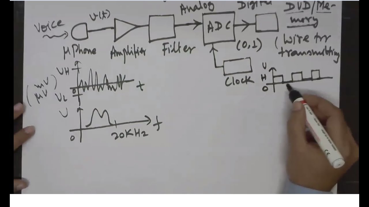
CMOS Analog Integrated Circuits - Lecture1: Introduction
CMOS Analog Integrated Circuits - Lecture1: Introduction
Related image with cmos analog integrated circuits lecture1 introduction


 – AICDESIGN.ORG")


 Analog CMOS Integrated Circuit Design Introduction And Backgroundsite.iugaza.edu.ps/jtaha ...")

Related image with cmos analog integrated circuits lecture1 introduction


")

About "Cmos Analog Integrated Circuits Lecture1 Introduction"
Comments are closed.