
Solved Consider The Following Circuit: Assume The Following | Chegg.com
Solved Consider The Following Circuit: Assume The Following | Chegg.com There are 2 steps to solve this one. consider the following circuit. assume r1 =5kΩ,r2 = 3ko,v cc= 10 v, and v dd= 15 v. note: this is a multi part question. Consider a silicon sample maintained at 300k under equilibrium conditions, uniformly doped with 1*1016 cm 3 phosphorus atoms. the surface region of the sample is additionally doped uniformly with 5*1016 cm 3 boron atoms, to a depth of 1 microm, as shown in the figure below.

Solved Consider The Following Circuit Assume The Following | Chegg.com
Solved Consider The Following Circuit Assume The Following | Chegg.com The circuit shown in the figure can be solved using ohm's law and the formula for calculating the total resistance in a series circuit. to find the current (i) flowing through the circuit, we can use the formula i = v/r, where v is the voltage and r is the total resistance. Consider the circuit shown in (figure 1). assume i = 0.88 a. what is the value of resistor r?. (4 points) problem 3: sequential circuit: consider the following circuit. assume that each inverter takes 1 time unit for a low to high or high to low transition. also assume that it takes 1 time unit for a pull up path or pull down path to pull up or pull down, respectively. Answer & explanation solved by verified expert rated helpful answered by thulasibukkana2145.

Solved Consider The Following Circuit And Answer The | Chegg.com
Solved Consider The Following Circuit And Answer The | Chegg.com (4 points) problem 3: sequential circuit: consider the following circuit. assume that each inverter takes 1 time unit for a low to high or high to low transition. also assume that it takes 1 time unit for a pull up path or pull down path to pull up or pull down, respectively. Answer & explanation solved by verified expert rated helpful answered by thulasibukkana2145. In the circuit, the source is replaced by a norton equivalent circuit consisting of a current v1 i1 = r1 in parallel with the resistor r1. this is necessary for the feedback analysis to conform to convention for shunt summing. Assume there is no channel length modulation.plot transconductance as vin is varied from 0 to 4 v . you only need to draw an approximate plot but markthe values clearly on the plot for the following 3 points: 1=0v,2 prob 2: consider the circuit shown below. the circuit has the following parameters: v d d = 4 v, r l. In an op amp, the negative feedback returns a fraction of the output to the inverting input terminal forcing the differential input to zero. since the op amp is ideal and has infinite gain, the differential input will exactly be zero. this is called a virtual short circuit. Consider the circuit shown in the figure. assume base to emitter voltage v be = 0.8 v and common base current gain (α) of the transistor is unity.

Solved Consider The Following Circuit: Assume The Following | Chegg.com
Solved Consider The Following Circuit: Assume The Following | Chegg.com In the circuit, the source is replaced by a norton equivalent circuit consisting of a current v1 i1 = r1 in parallel with the resistor r1. this is necessary for the feedback analysis to conform to convention for shunt summing. Assume there is no channel length modulation.plot transconductance as vin is varied from 0 to 4 v . you only need to draw an approximate plot but markthe values clearly on the plot for the following 3 points: 1=0v,2 prob 2: consider the circuit shown below. the circuit has the following parameters: v d d = 4 v, r l. In an op amp, the negative feedback returns a fraction of the output to the inverting input terminal forcing the differential input to zero. since the op amp is ideal and has infinite gain, the differential input will exactly be zero. this is called a virtual short circuit. Consider the circuit shown in the figure. assume base to emitter voltage v be = 0.8 v and common base current gain (α) of the transistor is unity.

Solved Consider The Following Circuit: Assume The Following | Chegg.com
Solved Consider The Following Circuit: Assume The Following | Chegg.com In an op amp, the negative feedback returns a fraction of the output to the inverting input terminal forcing the differential input to zero. since the op amp is ideal and has infinite gain, the differential input will exactly be zero. this is called a virtual short circuit. Consider the circuit shown in the figure. assume base to emitter voltage v be = 0.8 v and common base current gain (α) of the transistor is unity.
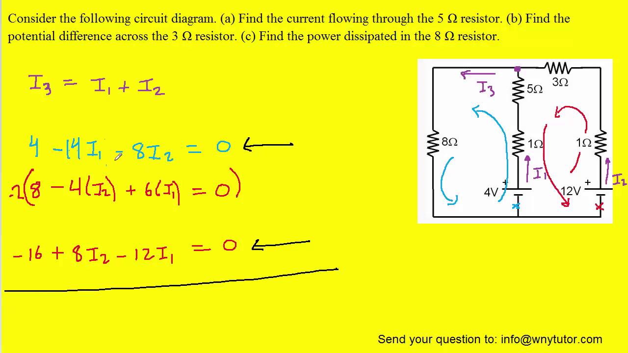
Consider the following circuit diagram
Consider the following circuit diagram
Related image with solved consider the following circuit and assume that the chegg com


Related image with solved consider the following circuit and assume that the chegg com


About "Solved Consider The Following Circuit And Assume That The Chegg Com"
Comments are closed.